| CPC H05K 1/0306 (2013.01) [C04B 37/026 (2013.01); H01L 23/15 (2013.01); H01L 23/3735 (2013.01); H05K 3/383 (2013.01)] | 17 Claims |
|
1. A bonded substrate comprising:
a silicon nitride ceramic substrate;
a bonding layer disposed over the silicon nitride ceramic substrate; and
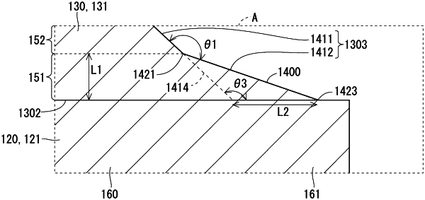
a copper plate disposed over the silicon nitride ceramic substrate, and having a first main surface, a second main surface, and an end surface, the second main surface being opposite the first main surface and bonded to the silicon nitride ceramic substrate by the bonding layer, the end surface extending from the first main surface to the second main surface, wherein
the end surface includes:
a first portion; and
a second portion closer to the second main surface than the first portion is,
the first portion and the second portion form an angle of 135° or more and 165° or less on an outside of the copper plate,
an extended plane of the first portion and the second main surface form an angle of 110° or more and 145° or less on a side where the second portion is located,
a distance from the second main surface to an intersection of the first portion and the second portion in a direction of a thickness of the copper plate is 10 μm or more and 100 μm or less, and
the second main surface extends beyond the extended plane of the first portion by a distance of 10 μm or more.
|