| CPC H05K 1/0224 (2013.01) [H01L 23/552 (2013.01); H05K 2201/0723 (2013.01)] | 20 Claims |
|
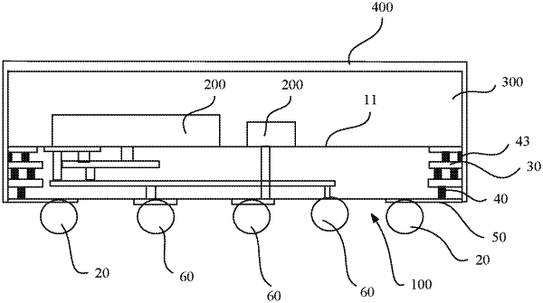
1. A shielding structure for a system-in-package, comprising:
a substrate, wherein the substrate comprises a first surface and an opposing second surface;
stacked first ground planes disposed in the substrate, wherein each first ground plane is disposed around an edge of the substrate;
a second ground plane disposed on the second surface, wherein the second ground plane surrounds an edge of the second surface, and wherein the second ground plane comprises a ring of ground pads arranged along the edge of the second surface;
a plurality of ground holes disposed in the substrate, wherein the ground holes are arranged along an edge of the substrate, wherein the ground holes comprise a first ground hole and a second ground hole, and wherein a diameter of the first ground hole is greater than a diameter of the second ground hole;
a first electrical coupling between adjacent first ground planes;
a second electrical coupling between the second ground plane and the first ground plane adjacent to the second ground plane, wherein the first electrical coupling and the second electrical coupling comprise the ground holes;
a device disposed on the first surface of the substrate, wherein the device comprises a package layer; and
a shield layer, wherein the shield layer wraps the package layer and extends to the substrate, and wherein the shield layer extends to the substrate and is electrically coupled to the first ground plane.
|