US 11,917,315 B2
Image sensor including CMOS image sensor pixel and dynamic vision sensor pixel
Yunjae Suh, Incheon (KR); Junseok Kim, Hwaseong-si (KR); Hyunsurk Ryu, Hwaseong-si (KR); Keun Joo Park, Seoul (KR); and Masamichi Ito, Hwaseong-si (JP)
Assigned to SAMSUNG ELECTRONICS CO., LTD., Suwon-si (KR)
Filed by SAMSUNG ELECTRONICS CO., LTD., Suwon-si (KR)
Filed on Jan. 23, 2023, as Appl. No. 18/100,392.
Application 18/100,392 is a continuation of application No. 17/492,059, filed on Oct. 1, 2021, granted, now 11,637,983.
Application 17/492,059 is a continuation of application No. 16/552,299, filed on Aug. 27, 2019, granted, now 11,140,349, issued on Oct. 5, 2021.
Claims priority of application No. 10-2018-0107280 (KR), filed on Sep. 7, 2018; and application No. 10-2019-0028938 (KR), filed on Mar. 13, 2019.
Prior Publication US 2023/0164461 A1, May 25, 2023
This patent is subject to a terminal disclaimer.
Int. Cl. H04N 25/75 (2023.01); H04N 25/77 (2023.01); H04N 25/47 (2023.01)
CPC H04N 25/75 (2023.01) [H04N 25/47 (2023.01); H04N 25/77 (2023.01)] 27 Claims
OG exemplary drawing
 
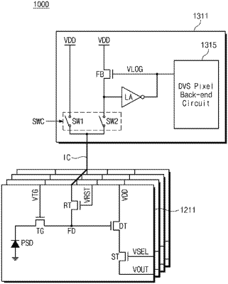
1. An image sensor comprising:
a photoelectric conversion device being responsive to an incident light;
a transfer transistor disposed between the photoelectric conversion device and a floating diffusion node and being responsive to a transfer control signal;
a reset transistor including a first electrode connected to the floating diffusion node and a gate electrode to receive a reset control signal; and
a switch circuitry configured to electrically connect a second electrode of the reset transistor either a power supply voltage or an event detect circuitry in response to a mode control signal.