| CPC H03M 1/1023 (2013.01) | 20 Claims |
|
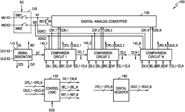
1. An analog-to-digital converter comprising:
a sample/hold circuit configured to sample a first input voltage and a second input voltage;
a digital-to-analog converter configured to output a first comparison voltage and a second comparison voltage based on the sampled first input voltage and the sampled second input voltage;
a plurality of comparison circuits configured to compare the first comparison voltage and the second comparison voltage to each other sequentially from a most significant bit to a least significant bit of a digital signal and output a plurality of comparison result signals;
a control logic configured to control an operation of the plurality of comparison circuits, and generate a plurality of reference signals based on the plurality of comparison result signals output from the plurality of comparison circuits; and
a digital register configured to output the digital signal based on the plurality of comparison result signals,
wherein the plurality of comparison circuits comprise:
a first comparison circuit configured to output a first comparison result signal in a first operation period;
a second comparison circuit configured to, in a second operation period after the first operation period, calibrate an offset of a second comparison result signal based on a first reference signal corresponding to the first comparison result signal from among the plurality of reference signals and output the calibrated second comparison result signal; and
a third comparison circuit configured to, in a third operation period after the second operation period, calibrate an offset of a third comparison result signal based on a second reference signal corresponding to the calibrated second comparison result signal from among the plurality of reference signals and output the calibrated third comparison result signal.
|