| CPC H03K 3/037 (2013.01) [H03K 3/012 (2013.01); H03K 3/0372 (2013.01)] | 12 Claims |
|
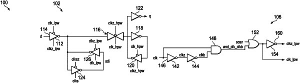
1. A flip-flop circuit comprising:
a first section configured to receive a primary clock signal, the first section being configured to generate a clock buffer signal having a series of pulses, each delayed by a set amount of time relative to a corresponding pulse of the primary clock signal, generate an intermediate clock signal based on the primary clock signal and the clock buffer signal, generate an inflated low pulse width clock signal having a low pulse width (LPW) that is greater than a low pulse width of the primary clock signal, and generate a complement inflated low pulse width clock signal;
a second section including at least one component configured to receive the inflated low pulse width clock signal and the complement inflated low pulse width clock signal; and
a third section configured to generate, based on the primary clock signal and the clock buffer signal, an inflated high pulse width clock signal having a high pulse width (HPW) that is greater than a high pulse width of the primary clock signal, and generate a complement inflated high pulse width clock signal,
wherein the second section includes a transmission gate configured to receive the inflated high pulse width clock signal and the complement inflated high pulse width clock signal.
|