| CPC H03K 17/063 (2013.01) [H03K 17/162 (2013.01); H03K 2217/0018 (2013.01)] | 4 Claims |
|
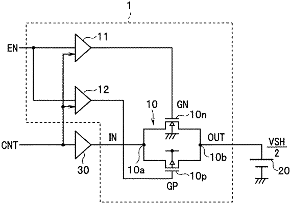
1. An analog switch circuit comprising:
an analog switch including an N-type MOSFET and a P-type MOSFET each having a gate operating withstand voltage of VGT, a source terminal of the N-type MOSFET and a source terminal of the P-type MOSFET being connected with each other, a drain terminal of the N-type MOSFET and a drain terminal of the P-type MOSFET being connected with each other, the N-type MOSFET and the P-type MOSFET being arranged in parallel, each of a potential of the drain terminal of the N-type MOSFET and a potential of the drain terminal of the P-type MOSFET being (VSH/2) when VSH is a voltage higher than VGT and equal to or lower than (2×VGT);
a first gate drive circuit to which an enable signal and a control signal are inputted, the first gate drive circuit being connected to a gate terminal of the N-type MOSFET of the analog switch; and
a second gate drive circuit to which the enable signal and the control signal are inputted, the second gate drive circuit being connected to a gate terminal of the P-type MOSFET of the analog switch, wherein
in a case where a logical value of the enable signal is 0,
a voltage 0 or a voltage VSH is applied to the source terminal of the N-type MOSFET of the analog switch and to the source terminal of the P-type MOSFET of the analog switch according to whether a logical value of the control signal is 0 or 1,
when the logical value of the control signal is 0, the first gate drive circuit outputs a signal of voltage 0 to the gate terminal of the N-type MOSFET, and the second gate drive circuit outputs a signal of voltage (VSH/2) to the gate terminal of the P-type MOSFET, and
when the logical value of the control signal is 1, the first gate drive circuit outputs a signal of voltage (VSH/2) to the gate terminal of the N-type MOSFET, and the second gate drive circuit outputs a signal of voltage VSH to the gate terminal of the P-type MOSFET.
|