| CPC H03F 1/0211 (2013.01) [H03F 3/45197 (2013.01); H03M 1/66 (2013.01); H03F 2200/375 (2013.01); H03F 2203/45044 (2013.01)] | 20 Claims |
|
1. A circuit comprising:
a reference circuit comprising a first reference voltage node and a second reference voltage node;
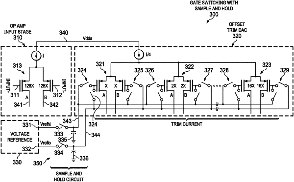
a digital-to-analog conversion (DAC) circuit comprising a plurality of transistor pairs, wherein each transistor pair of the plurality of transistor pairs comprises a first transistor and a second transistor, wherein a source terminal of the first transistor is coupled to a source terminal of the second transistor, wherein a gate terminal of the first transistor is coupled to a first pair of switches, wherein a gate terminal of the second transistor is coupled to a second pair of switches, wherein a first switch of the first pair of switches is coupled to a first node, wherein a second switch of the first pair of switches is coupled to a second node, wherein a first switch of the second pair of switches is coupled to the first node, wherein a second switch of the second pair of switches is coupled to the second node;
a third switch coupled to the first node and to the first reference voltage node; and
a fourth switch coupled to the second node and to the second reference voltage node.
|