| CPC H02M 1/08 (2013.01) | 6 Claims |
|
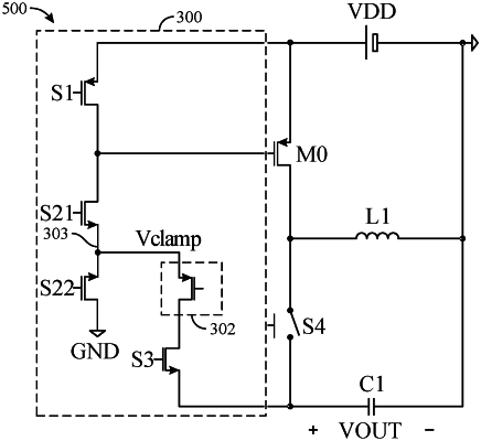
1. A power supply circuit comprising:
a switching converter having a switching transistor having a source coupled to a first voltage rail; and
a gate driver having an output coupled to a gate of the switching transistor, the gate driver comprising:
a first switching device coupled between the output of the gate driver and the first voltage rail;
a second switching device coupled between the output of the gate driver and a voltage node of the gate driver;
a third switching device coupled between the voltage node of the gate driver and a second voltage rail; and
a voltage clamp coupled in series with a fourth switching device, the voltage clamp and the fourth switching device being coupled between a third voltage rail and the voltage node, wherein:
the switching transistor is a p-type transistor;
the first voltage rail has a first voltage;
the second voltage rail has a second voltage lower than the first voltage; and
the third voltage rail has a third voltage lower than the second voltage.
|