| CPC H01Q 9/0407 (2013.01) [G01S 13/767 (2013.01); H01Q 1/2283 (2013.01); H01Q 1/48 (2013.01); H01Q 21/065 (2013.01)] | 20 Claims |
|
1. An electronic device comprising:
a housing comprising:
a front surface plate forming a front surface of the electronic device,
a rear surface plate forming a rear surface of the electronic device, and
a side surface member forming a side surface of the electronic device;
a printed circuit board positioned within the housing and having at least one electronic component disposed thereon;
a first support structure positioned between the printed circuit board and the rear surface plate, and formed with a conductive material;
a second support structure disposed adjacent to the first support structure and formed with a nonconductive material;
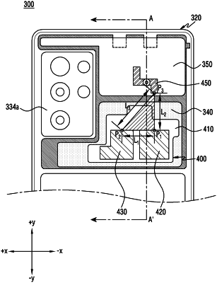
a patch antenna comprising:
a flexible printed circuit board disposed on one surface of the first support structure that faces the rear surface plate,
a first conductive patch disposed on the flexible printed circuit board, and
a second conductive patch disposed to be spaced apart from the first conductive patch;
a conductive pattern disposed on one surface of the second support structure that faces the rear surface plate; and
a wireless communication circuit electrically connected with the first conductive patch, the second conductive patch, and the conductive pattern,
wherein the first conductive patch is fed from the wireless communication circuit at a first point,
wherein the second conductive patch is fed from the wireless communication circuit at a second point, and
wherein the conductive pattern is fed from the wireless communication circuit at a third point.
|