| CPC H01L 33/58 (2013.01) [H01L 27/156 (2013.01); H01L 33/382 (2013.01); H01L 33/50 (2013.01)] | 20 Claims |

|
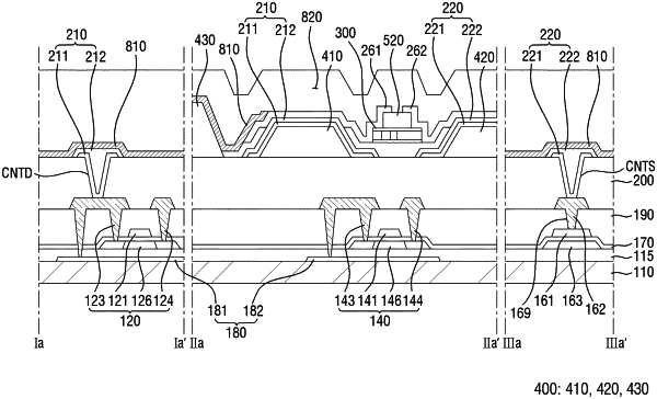
1. A display device comprising:
a first electrode and a second electrode that are spaced apart from and face each other;
a light-blocking layer disposed on the first electrode and the second electrode; and
at least one light-emitting element disposed between the first electrode and the second electrode, wherein
the light-blocking layer includes:
a light-blocking portion absorbing light; and
at least one opening pattern,
the light-blocking portion includes an area partially overlapping the first electrode and the second electrode,
the at least one opening pattern exposes portions of the first and second electrodes facing each other and exposes at least a portion of an area between the first and second electrodes facing each other, and
the at least one light-emitting element overlaps the at least one opening pattern.
|