| CPC H01L 33/44 (2013.01) [H01L 25/0753 (2013.01); H01L 33/20 (2013.01); H01L 33/38 (2013.01); H01L 33/507 (2013.01); H01L 33/60 (2013.01); H01L 33/62 (2013.01)] | 19 Claims |
|
1. A display device, comprising:
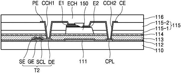
a substrate;
a thin-film transistor and a common power line disposed on the substrate;
a passivation layer disposed on the thin-film transistor and the common power line;
a light-emitting device disposed on the passivation layer and including a first electrode, a second electrode, and a structure disposed between the first electrode and the second electrode;
a planarization layer disposed on the passivation layer to cover a side surface of the light-emitting device;
a pixel electrode electrically connected to the thin-film transistor through a first circuit contact hole in the passivation layer and the planarization layer, and electrically connected to the first electrode through an electrode contact hole in the planarization layer; and
a common electrode electrically connected to the common power line through a second circuit contact hole formed in the passivation layer and planarization layer, and electrically connected to the second electrode through the electrode contact hole formed in the planarization layer.
|