| CPC H01L 29/78618 (2013.01) [H01L 28/56 (2013.01); H01L 28/57 (2013.01); H01L 28/60 (2013.01); H01L 28/65 (2013.01); H01L 29/2003 (2013.01); H01L 29/6684 (2013.01); H01L 29/7375 (2013.01); H01L 29/7408 (2013.01); H01L 29/7869 (2013.01); H10B 53/30 (2023.02); H10B 12/312 (2023.02); H10B 12/36 (2023.02)] | 18 Claims |
|
1. A semiconductor device, comprising:
a transistor formed on a silicon substrate;
a capacitor electrically connected to the transistor by a conductive via, the capacitor comprising:
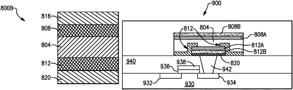
upper and lower conductive oxide electrodes on opposing sides of a polar layer, wherein the lower conductive oxide electrode is electrically connected to a drain of the transistor, and
the polar layer comprising a base polar material doped with a dopant, wherein the base polar material includes one or more metal elements and one or both of oxygen or nitrogen, and wherein the dopant comprises a metal element of one of 4d series, 5d series, 4f series or 5f series that is different from the one or more metal elements and is present at a concentration such that a remnant polarization of the polar layer is different than that of the base polar material without the dopant,
wherein the polar layer has a perovskite crystal structure and the dopant occupies a corner site of a unit cell of the perovskite crystal structure; and
a barrier sealant layer formed on one or both side surfaces of one or more of the polar layer, the upper conductive oxide electrode layer and the lower conductive oxide electrode layer.
|