US 11,916,132 B2
Semiconductor device and method of manufacture
Wan-Yi Kao, Baoshan Township (TW); Hung Cheng Lin, Hsinchu (TW); Che-Hao Chang, Hsinchu (TW); Yung-Cheng Lu, Hsinchu (TW); and Chi On Chui, Hsinchu (TW)
Assigned to Taiwan Semiconductor Manufacturing Co., Ltd., Hsinchu (TW)
Filed by Taiwan Semiconductor Manufacturing Co., Ltd., Hsinchu (TW)
Filed on Jun. 30, 2022, as Appl. No. 17/854,599.
Application 17/854,599 is a continuation of application No. 17/072,719, filed on Oct. 16, 2020, granted, now 11,437,492.
Claims priority of provisional application 63/027,618, filed on May 20, 2020.
Prior Publication US 2022/0336637 A1, Oct. 20, 2022
This patent is subject to a terminal disclaimer.
Int. Cl. H01L 29/66 (2006.01); H01L 21/02 (2006.01); H01L 29/06 (2006.01); H01L 29/423 (2006.01); H01L 29/49 (2006.01); H01L 29/786 (2006.01)
CPC H01L 29/66553 (2013.01) [H01L 21/02167 (2013.01); H01L 21/02211 (2013.01); H01L 21/0228 (2013.01); H01L 21/02603 (2013.01); H01L 29/0673 (2013.01); H01L 29/42392 (2013.01); H01L 29/4983 (2013.01); H01L 29/66742 (2013.01); H01L 29/78696 (2013.01)] 20 Claims
OG exemplary drawing
 
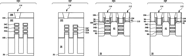
1. A semiconductor device comprising:
a plurality of nanostructures surrounded by a gate dielectric, wherein each one of the plurality of nanostructures has a constant thickness; and
an inner spacer extending between adjacent ones of the plurality of nanostructures, the inner spacer having a dished surface, the dished surface having a depth of less than about 4.3 nm.