| CPC H01L 29/42392 (2013.01) [H01L 29/0847 (2013.01); H01L 29/78696 (2013.01)] | 18 Claims |
|
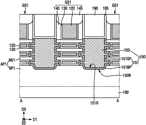
1. A semiconductor device, comprising:
an active pattern which includes a lower pattern, and a plurality of sheet patterns spaced apart from the lower pattern in a first direction;
a gate structure which is placed on the lower pattern, and includes a gate electrode which surrounds the plurality of sheet patterns; and
a source/drain pattern located on both sides of the gate structure;
wherein the source/drain pattern includes a silicon-germanium liner being in contact with each of the sheet patterns and the lower pattern, and a filling semiconductor pattern placed on the silicon-germanium liner;
wherein the filling semiconductor pattern includes silicon doped with an n-type first impurity;
wherein the source/drain pattern further includes an insertion liner pattern, which extends between the silicon-germanium liner and the filling semiconductor pattern and extends along a profile of the silicon-germanium liner; and
wherein the insertion liner pattern includes silicon doped with an n-type second impurity different from the first impurity.
|