| CPC H01L 29/1608 (2013.01) [C30B 23/02 (2013.01); C30B 29/36 (2013.01); H01L 29/7827 (2013.01); H01L 29/04 (2013.01); H01L 29/0696 (2013.01); H01L 29/4236 (2013.01); H01L 29/66068 (2013.01)] | 20 Claims |
|
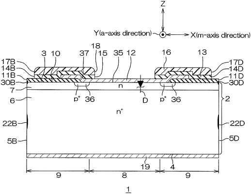
1. An SiC semiconductor device comprising:
an SiC semiconductor layer including an SiC monocrystal and having a first main surface as a device surface, a second main surface at a side opposite to the first main surface, and a side surface connecting the first main surface and the second main surface;
a main surface insulating layer including an insulating material, covering the first main surface of the SiC semiconductor layer, and having an insulating side surface formed flush with respect to the side surface of the SiC semiconductor layer; and
a boundary modified layer including a first region that is modified to be of a property differing from the SiC monocrystal and a second region that is modified to be of a property differing from the insulating material, and being formed across the side surface of the SiC semiconductor layer and the insulating side surface of the main surface insulating layer,
wherein the boundary modified layer is exposed outside from the side surface of the SiC semiconductor layer and the insulating side surface of the main surface insulating layer.
|