US 11,916,076 B2
Device disaggregation for improved performance
Javier A. Delacruz, San Jose, CA (US); Don Draper, San Jose, CA (US); Jung Ko, San Jose, CA (US); and Steven L. Teig, Menlo Park, CA (US)
Assigned to Adeia Semiconductor Inc., San Jose, CA (US)
Filed by Adeia Semiconductor Inc., San Jose, CA (US)
Filed on Jun. 29, 2020, as Appl. No. 16/915,140.
Application 16/915,140 is a continuation of application No. 16/156,506, filed on Oct. 10, 2018, granted, now 10,700,094.
Claims priority of provisional application 62/715,966, filed on Aug. 8, 2018.
Prior Publication US 2020/0403006 A1, Dec. 24, 2020
Int. Cl. H01L 25/065 (2023.01); H01L 25/00 (2006.01); H01L 27/118 (2006.01)
CPC H01L 27/11807 (2013.01) [H01L 25/0652 (2013.01); H01L 25/0657 (2013.01); H01L 25/50 (2013.01); H01L 2027/11838 (2013.01); H01L 2027/11875 (2013.01); H01L 2027/11879 (2013.01); H01L 2027/11881 (2013.01)] 32 Claims
OG exemplary drawing
 
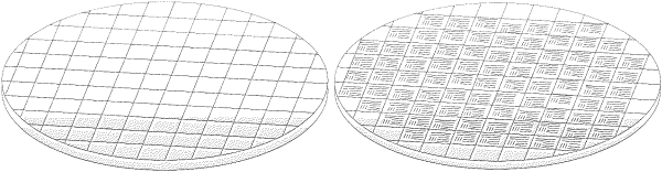
1. A method of manufacturing a programmable logic device from disaggregated device components, the method comprising:
forming one or more routing layers on a wafer; and
hybrid bonding one or more dies comprising logic components to the wafer to form, via the one or more routing layers, a plurality of routing paths communicatively coupling at least some of the logic components of the one or more dies to one another to form the programmable logic device.