| CPC H01L 27/0922 (2013.01) [H01L 21/761 (2013.01); H01L 21/76224 (2013.01); H01L 21/823878 (2013.01); H01L 21/823481 (2013.01); H01L 21/823892 (2013.01); H01L 29/7813 (2013.01)] | 4 Claims |
|
1. An integrated circuit (IC) structure, comprising:
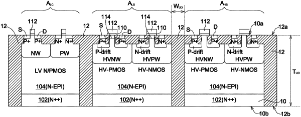
a substrate having a top surface and a bottom surface oppositely, and the substrate comprising a plurality of regions;
semiconductor devices formed at the substrate and respectively within the plurality of regions; and
an UD trench isolation structure formed in the substrate and surrounding peripheries of each of the plurality of regions for isolating the semiconductor devices within different regions of the plurality of regions;
wherein the UD trench isolation structure penetrates the substrate in its entirety by extending from the top surface to the bottom surface, and a lower surface of the UD trench isolation structure is exposed at the bottom surface;
wherein the plurality of regions comprises a high-side region, a low-side region, a first region and a second region apart from each other by the UD trench isolation structure; and peripheries of the high-side region, the low-side region, the first region and the second region are surrounded by the UD trench isolation structure, wherein the high-side region, the low-side region, the first region and the second region are adjacent to each other;
wherein a first vertical double-diffused metal oxide semiconductor (VDMOS) transistor is formed in the first region; a second VDMOS transistor is formed in the second region; and a first drain region of the first VDMOS transistor is apart from a second drain region of the second VDMOS transistor by the UD trench isolation structure.
|