| CPC H01L 27/0886 (2013.01) [H01L 21/823418 (2013.01); H01L 21/823431 (2013.01); H01L 21/823468 (2013.01); H01L 21/823821 (2013.01); H01L 21/845 (2013.01); H01L 27/0924 (2013.01); H01L 27/1211 (2013.01); H01L 29/0649 (2013.01); H01L 29/7848 (2013.01)] | 20 Claims |
|
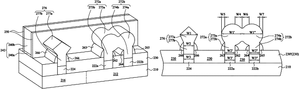
1. A device comprising:
a first semiconductor fin on a substrate;
a second semiconductor fin next to the first semiconductor fin, the first semiconductor fin having a first side facing the second semiconductor fin and a second side facing away from the second semiconductor fin, the second semiconductor fin having a first side facing the first semiconductor fin and a second side facing away from the first semiconductor fin;
a first epitaxy structure on the first semiconductor fin, wherein the first epitaxy structure laterally extends a first width from the first side of the first semiconductor fin toward the second semiconductor fin, and a second width from the second side of the first semiconductor fin in a direction away from the second semiconductor fin, and the first width of the first epitaxy structure is greater than the second width of the first epitaxy structure;
a second epitaxy structure on the second semiconductor fin, wherein the second epitaxy structure laterally extends a first width from the first side of the second semiconductor fin toward the first semiconductor fin, and a second width from the second side of the second semiconductor fin in a direction away from the first semiconductor fin, and the first width of the second epitaxy structure is greater than the second width of the second epitaxy structure;
a first fin sidewall spacer adjacent the first side of the first semiconductor fin; and
a second fin sidewall spacer adjacent the second side of the first semiconductor fin and having a top end higher than a top end of the first fin sidewall spacer.
|