| CPC H01L 27/0629 (2013.01) [H01L 27/0605 (2013.01)] | 13 Claims |
|
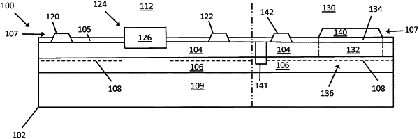
1. A semiconductor device, comprising:
a semiconductor die comprising a barrier layer of type III-V semiconductor material, a channel layer of type III-V semiconductor material disposed below the barrier layer, the channel layer forming a heterojunction with the barrier layer such that a two-dimensional charge carrier gas is disposed in the channel layer near the heterojunction; and
a capacitor monolithically formed in the semiconductor die,
wherein a dielectric medium of the capacitor comprises a first section of the barrier layer.
|