| CPC H01L 27/0251 (2013.01) [H01L 21/28052 (2013.01); H01L 21/28097 (2013.01); H01L 21/28518 (2013.01); H01L 29/0649 (2013.01); H01L 29/4933 (2013.01); H01L 29/66659 (2013.01)] | 20 Claims |

|
1. A method for forming a semiconductor device, the method comprising:
forming a gate stack over a semiconductor substrate;
forming a source region in the semiconductor substrate and on a first side of the gate stack;
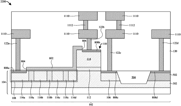
forming a drain region comprising a plurality of drain segments, wherein the drain region is formed in the semiconductor substrate and on a second side of the gate stack opposite the first side, and wherein forming the drain region comprises:
forming a patterned masking layer over the semiconductor substrate, wherein the patterned masking layer comprises a plurality of openings disposed on the second side of the gate stack; and
implanting first doping type dopants into the semiconductor substrate through the plurality of openings of the patterned masking layer to form the plurality of drain segments individual to and respectively underlying the plurality of openings;
forming a silicide blocking layer over the semiconductor substrate, wherein the silicide blocking layer at least partially covers the drain region;
with the silicide blocking layer in place over the semiconductor substrate, performing a silicide process on the semiconductor substrate to form a silicide structure partially over the drain region; and
forming a conductive contact overlying the drain region;
wherein the plurality of drain segments are spaced from each other after the forming of the conductive contact, wherein the plurality of drain segments comprise a distal drain segment that is farthest from the gate stack amongst the plurality of drain segments, wherein the conductive contact overlies the distal drain segment, and wherein a remainder of the plurality of drain segments are completely covered by the silicide blocking layer after the forming of the conductive contact.
|