| CPC H01L 25/167 (2013.01) [H01L 33/62 (2013.01); G09G 3/32 (2013.01)] | 11 Claims |
|
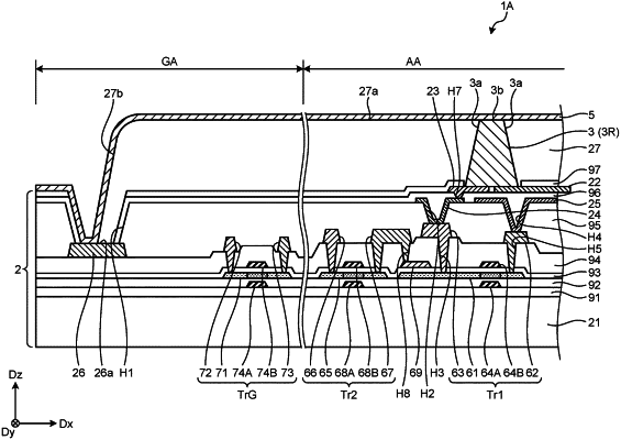
1. A display device comprising:
a substrate;
a plurality of pixels arrayed on the substrate and configured to display different colors;
an inorganic light-emitting element provided to each of the pixels;
a flattening film that surrounds at least a side surface of the inorganic light-emitting element; and
an inorganic film that covers the flattening film and the inorganic light-emitting element
a transistor provided to a first surface of the substrate;
an insulating film that covers the transistor; and
cathode wiring provided to the first surface of the substrate and electrically coupled to a cathode of the inorganic light-emitting element,
wherein
the flattening film and the inorganic film are provided on an upper side of the insulating film from a display region provided with a plurality of the inorganic light-emitting elements to a peripheral region positioned outside the display region,
the cathode wiring is exposed at a bottom of a contact hole formed in the peripheral region of the insulating film, and
the inorganic film covers a side surface of the flattening film and is in contact with the cathode wiring at the bottom of the contact hole.
|