| CPC H01L 25/0657 (2013.01) [H01L 24/32 (2013.01); H01L 24/48 (2013.01); H01L 24/73 (2013.01); H01L 2224/32145 (2013.01); H01L 2224/32225 (2013.01); H01L 2224/48145 (2013.01); H01L 2224/48227 (2013.01); H01L 2224/73265 (2013.01); H01L 2225/0651 (2013.01); H01L 2225/06506 (2013.01); H01L 2225/06562 (2013.01); H01L 2924/00014 (2013.01)] | 20 Claims |
|
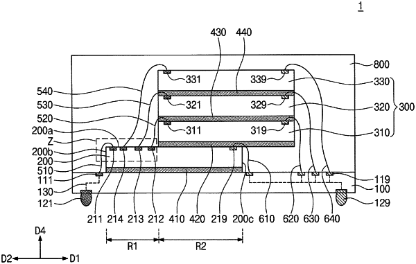
1. A semiconductor package, comprising:
a substrate;
a lower semiconductor chip on the substrate, the lower semiconductor chip having a first region and a second region in a plan view;
a first upper semiconductor chip on a top surface of the second region of the lower semiconductor chip and exposing a top surface of the first region of the lower semiconductor chip;
a second upper semiconductor chip on the first upper semiconductor chip;
a first signal bonding wire on the top surface of the first region of the lower semiconductor chip and coupled to the first upper semiconductor chip and the lower semiconductor chip;
a first ground bonding wire on a top surface of the first upper semiconductor chip and coupled to the substrate, the first ground bonding wire being spaced apart from the lower semiconductor chip; and
a second ground bonding wire on a top surface of the second upper semiconductor chip and coupled to the substrate, the second ground bonding wire being spaced apart from the lower semiconductor chip and the first upper semiconductor chip,
wherein the first ground bonding wire and the second ground bonding wire are electrically isolated from the lower semiconductor chip.
|