US 11,916,024 B2
Semiconductor devices comprising steps
Rohit Kothari, Boise, ID (US); Adam L Olson, Boise, ID (US); John D. Hopkins, Meridian, ID (US); and Jeslin J. Wu, Boise, ID (US)
Assigned to Micron Technology, Inc., Boise, ID (US)
Filed by Micron Technology, Inc., Boise, ID (US)
Filed on Sep. 14, 2021, as Appl. No. 17/447,618.
Application 17/447,618 is a division of application No. 16/235,665, filed on Dec. 28, 2018, granted, now 11,127,691.
Prior Publication US 2021/0407930 A1, Dec. 30, 2021
Int. Cl. H01L 23/00 (2006.01); H01L 21/3105 (2006.01); H01L 21/311 (2006.01); H01L 21/762 (2006.01)
CPC H01L 23/562 (2013.01) [H01L 21/31053 (2013.01); H01L 21/31144 (2013.01); H01L 21/76224 (2013.01)] 24 Claims
OG exemplary drawing
 
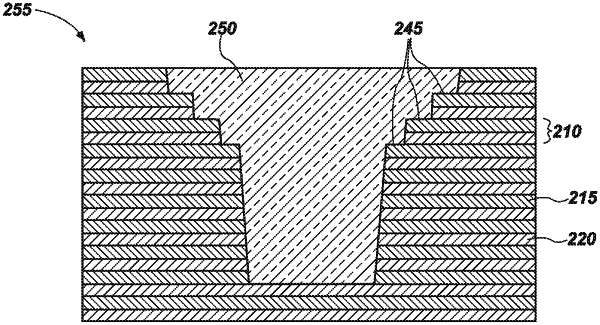
1. A semiconductor device, comprising:
a stack of materials comprising:
tiers; and
opposing steps in a portion of the stack of materials, the opposing steps each defined by opposing sidewalls of the stack of materials and defined by a respective riser portion having a riser height greater than twice a height of one of the tiers;
a dielectric material between the opposing sidewalls of the stack of materials; and
at least one semiconductor feature adjacent the stack of materials.