| CPC H01L 23/49822 (2013.01) [H01L 23/3157 (2013.01); H01L 23/49811 (2013.01); H01L 23/5389 (2013.01); H01L 24/08 (2013.01); H01L 25/18 (2013.01); H01L 2224/08235 (2013.01)] | 20 Claims |
|
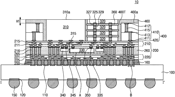
1. A semiconductor package, comprising:
a package substrate;
an interposer substrate on the package substrate, the interposer substrate including a first redistribution substrate, a second redistribution substrate below a bottom surface of the first redistribution substrate, and an interposer molding layer between the first redistribution substrate and the second redistribution substrate;
a connection substrate on the interposer substrate, the connection substrate having a connection hole that penetrates through the connection substrate;
a first semiconductor chip on the interposer substrate within the connection hole;
a second semiconductor chip on the interposer substrate within the connection hole and horizontally spaced apart from the first semiconductor chip;
a molding layer disposed between the first semiconductor chip, the second semiconductor chip, and the connection substrate and covering a sidewall of the first semiconductor chip, a sidewall of the second semiconductor chip, and the connection substrate; and
a connection semiconductor chip in the interposer molding layer and on the bottom surface of the first redistribution substrate.
|