| CPC H01L 21/823487 (2013.01) [H01L 21/823437 (2013.01); H01L 21/823481 (2013.01)] | 15 Claims |
|
1. A method of forming an integrated circuit device, the method comprising:
forming a lower structure on a substrate, the lower structure comprising:
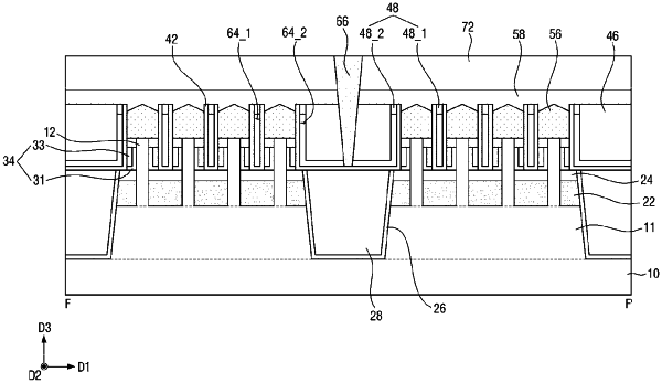
a first vertical field-effect transistor (VFET) and a second VFET on the substrate, wherein each of the first VFET and the second VFET comprises a bottom source/drain region in the substrate, a channel region and a top source/drain region that are sequentially stacked on the substrate in a vertical direction, and a gate structure on a side surface of the channel region;
a preliminary isolation structure between the first VFET and the second VFET, wherein the preliminary isolation structure comprises a sacrificial layer and a gap capping layer sequentially stacked on the substrate in the vertical direction; and
a gate liner on opposing sides of the preliminary isolation structure and between the preliminary isolation structure and the substrate;
forming a top capping layer on the lower structure; and then
forming a cavity between the first WET and the second WET by removing the sacrificial layer,
wherein the forming the cavity comprises a performing a wet etching process until the gate liner is exposed.
|