| CPC H01L 21/6835 (2013.01) [H10K 50/8426 (2023.02); H10K 50/856 (2023.02); H10K 59/122 (2023.02); H10K 71/00 (2023.02); H01L 2221/6835 (2013.01); H01L 2221/68386 (2013.01)] | 20 Claims |
|
1. A method of manufacturing a high resolution micro-LED display panel, wherein the method comprises following steps:
providing a driving backplane and a light-emitting substrate, and bonding the driving backplane and the light-emitting substrate;
patterning the light-emitting substrate to form a pixel array;
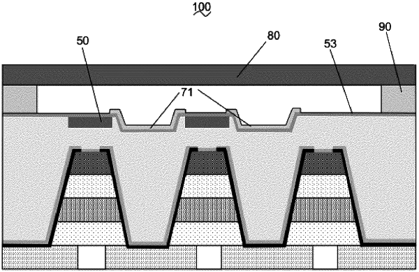
forming a thin film packaging layer on an outside of the pixel array, the thin film packaging layer completely covering the pixel array;
forming quantum dots on the top of the thin film packaging layer to form a multi-color display;
forming a reflective array between two adjacent quantum dots to avoid optical crosstalk between the pixel arrays;
wherein a pixel definition layer is provided on a top surface of the thin film packaging layer, and the quantum dots are formed in said pixel definition layer.
|