| CPC H01L 21/67248 (2013.01) [C23C 16/482 (2013.01); H01J 37/3299 (2013.01); H01J 37/32449 (2013.01); H01J 37/32724 (2013.01); H01J 37/32917 (2013.01); H01J 37/32935 (2013.01); H01J 37/32972 (2013.01); H01L 21/67069 (2013.01); H01L 21/67098 (2013.01); H01L 21/67115 (2013.01); H01L 21/67207 (2013.01); H01L 22/12 (2013.01); H01L 22/20 (2013.01); H01J 2237/2001 (2013.01); H01J 2237/24585 (2013.01); H01J 2237/334 (2013.01)] | 5 Claims |
|
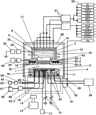
1. A method of processing a semiconductor wafer comprising:
locating the semiconductor wafer on an upper surface of a sample stage disposed in a lower portion of a processing chamber inside a vessel;
supplying a process gas into the processing chamber;
absorbing particles generated by the process gas on a film disposed on an upper surface of the wafer to generate a product layer;
desorbing the product layer, after the absorbing step, by heating the wafer using infrared (IR) light emitted from a lamp disposed above the sample stage;
detecting IR light exiting from a rear surface of the wafer from an upper and out of a rear surface thereof, during a period in which the emission of the IR light by the lamp is lowered so that the product layer is not desorbed, after having passed through an inside of the semiconductor wafer, using a detector disposed below the upper surface of the sample stage, and detecting a characteristic change of intensities of the IR light in a plurality of wavelengths thereof;
determining a temperature of the semiconductor wafer using a result of detecting a wavelength of the IR light in which the characteristic change occurred and data which is obtained before the processing of the semiconductor wafer and indicating a relationship between the temperature of the semiconductor wafer and the wavelength of the IR light in which the characteristic change occurred; and
adjusting the temperature of the semiconductor wafer using the value obtained by the step of determining the temperature of the semiconductor wafer.
|