US 11,915,938 B2
Method of manufacturing semiconductor device, substrate processing apparatus, and recording medium
Arito Ogawa, Toyama (JP); and Atsuro Seino, Toyama (JP)
Assigned to Kokusai Electric Corporation, Tokyo (JP)
Filed by KOKUSAI ELECTRIC CORPORATION, Tokyo (JP)
Filed on Dec. 21, 2022, as Appl. No. 18/085,970.
Application 18/085,970 is a continuation of application No. 16/800,744, filed on Feb. 25, 2020, granted, now 11,538,688.
Application 16/800,744 is a continuation of application No. PCT/JP2018/011719, filed on Mar. 23, 2018.
Claims priority of application No. 2017-183406 (JP), filed on Sep. 25, 2017.
Prior Publication US 2023/0131197 A1, Apr. 27, 2023
Int. Cl. H01L 21/285 (2006.01); C23C 16/34 (2006.01); C23C 16/52 (2006.01); H01L 21/768 (2006.01); C23C 16/455 (2006.01); C23C 16/458 (2006.01); H01L 21/28 (2006.01); H01L 21/02 (2006.01); C23C 16/44 (2006.01)
CPC H01L 21/28568 (2013.01) [C23C 16/34 (2013.01); C23C 16/52 (2013.01)] 17 Claims
OG exemplary drawing
 
1. A method of processing a substrate, comprising:
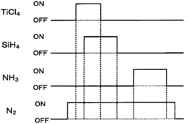
forming a metal-containing film on the substrate by sequentially performing:
(a) supplying a first gas, which contains a metal and a halogen, and a first reducing gas, which contains silicon and hydrogen and does not contain a halogen, to the substrate in a process chamber by setting an internal pressure of the process chamber to a value in a predetermined pressure range, wherein (a) includes a time period of simultaneously supplying the first gas and the first reducing gas and a time period of supplying the first gas;
(b) removing the first gas and the first reducing gas that remain in the process chamber;
(c) supplying a second gas to the substrate; and
(d) removing the second gas remaining in the process chamber.