| CPC H01L 21/0337 (2013.01) [H01L 21/0274 (2013.01); H01L 21/0332 (2013.01); H01L 21/31144 (2013.01)] | 20 Claims |

|
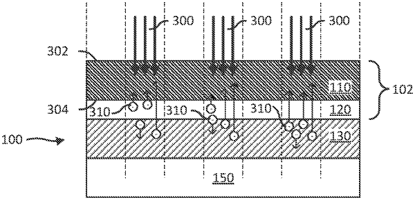
1. A method for fabricating a semiconductor device comprising:
forming a base layer over a top layer of a substrate, the base layer comprising a silicon based dielectric having a thickness less than or equal to 5 nm and greater than or equal to 0.5 nm;
forming a photoresist layer over the base layer, the photoresist comprising a first side and an opposite second side;
exposing a first portion of the photoresist layer to a pattern of extreme ultraviolet (EUV) radiation from the first side;
exposing a second portion of the photoresist layer with a pattern of electron flux from the second side, the electron flux being directed into the photoresist layer from the base layer in response to the EUV radiation;
developing the exposed photoresist layer to form a patterned photoresist layer; and
transferring the pattern of the patterned photoresist layer to the base layer and the top layer.
|
|
12. A method for forming an etch mask over a substrate, the method comprising:
forming an electron booster layer adhering to a major surface of the substrate;
exposing the major surface of the electron booster layer to a hydrogen-containing gas to convert the major surface be hydrophobic;
forming a photoresist layer adhering to the hydrophobic major surface of the electron booster layer;
exposing a first portion of the photoresist layer with a pattern of extreme ultraviolet (EUV) radiation;
exposing a second portion of the photoresist layer with electron flux directed from the electron booster layer, wherein a portion of the EUV radiation is absorbed below the photoresist layer to generate the electron flux;
developing the exposed photoresist layer to form a patterned photoresist layer; and
patterning the electron booster layer with the patterned photoresist layer to form a patterned electron booster layer, the etch mask being the combined patterned electron booster layer and the patterned photoresist layer remaining after patterning the electron booster layer.
|
|
16. A method for patterning a substrate comprising:
preparing a plurality of test substrates, wherein each test substrates has a substantially same top layer;
forming a lithography stack over the top layer of each of the plurality of test substrates, the lithography stack comprising a base layer and a photoresist layer disposed over the base layer, wherein the base layer in each of the plurality of test substrates has a different combination of thickness and composition;
patterning each photoresist layer with an extreme ultraviolet (EUV) lithography process, by exposing the photoresist layer to a pattern of EUV radiation in a focus-exposure matrix;
obtaining patterning metrics by measuring the patterned photoresist layer of each of the plurality of test substrates; and
based on the patterning metrics, selecting a first type of base layer, the first type of base layer having a specific combination of a first thickness and a first composition for forming a first base layer of a lithography stack for an EUV lithography process.
|