| CPC H01L 21/02532 (2013.01) [H01L 21/0217 (2013.01); H01L 21/02164 (2013.01); H01L 21/8221 (2013.01); H01L 29/263 (2013.01); H10B 41/10 (2023.02); H10B 41/27 (2023.02); H10B 41/35 (2023.02); H10B 43/10 (2023.02); H10B 43/35 (2023.02)] | 7 Claims |
|
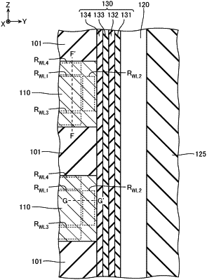
1. A semiconductor memory device comprising:
a plurality of conductive layers and a plurality of interlayer insulating layers alternately arranged in a first direction;
a semiconductor layer extending in the first direction and being opposed to the plurality of conductive layers; and
a gate insulating film disposed between the plurality of conductive layers and the semiconductor layer, wherein
the plurality of interlayer insulating layers include a first interlayer insulating layer and a second interlayer insulating layer adjacent in the first direction, and
the plurality of conductive layers include a first conductive layer disposed between the first interlayer insulating layer and the second interlayer insulating layer, wherein
the first conductive layer includes:
a first region;
a second region disposed between the first region and the gate insulating film; and
a third region disposed between the first region and the first interlayer insulating layer, wherein
the first region to the third region contain a metal,
the third region contains silicon (Si),
the first region does not contain silicon (Si) or has a lower silicon (Si) content than a silicon (Si) content in the third region, and
the second region does not contain silicon (Si) or has a lower silicon (Si) content than the silicon (Si) content in the third region.
|