| CPC H01L 21/02164 (2013.01) [B81B 7/0035 (2013.01); B81B 7/0061 (2013.01); B81C 1/00293 (2013.01); B81C 1/00349 (2013.01); H01L 21/31111 (2013.01); H01L 23/08 (2013.01); H01L 23/10 (2013.01); H01L 29/84 (2013.01); B81B 2201/02 (2013.01); B81C 2201/019 (2013.01); B81C 2203/03 (2013.01); G01P 15/0802 (2013.01); G01P 15/125 (2013.01)] | 7 Claims |
|
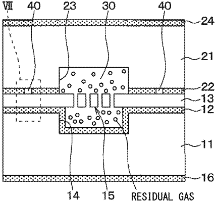
1. A semiconductor device having a space therein, comprising:
a support layer made of silicon;
an activation layer made of silicon, having an element portion, and bonded to the support layer via a first silicon oxide film layer; and
a cap portion made of silicon, bonded to the activation layer via a second silicon oxide film layer, and having a recess disposed at a position corresponding to the element portion, wherein:
the support layer, the first silicon oxide film layer, the activation layer, the second silicon oxide film layer, and the cap portion provide a stacking structure, and the recess provides the space inside the stacking structure, the semiconductor device further comprising:
a gas discharge passage only arranged in one of the first silicon oxide film layer sandwiched between the support layer and the activation layer and the second silicon oxide film layer sandwiched between the activation layer and the cap portion, surrounding the space, and reaching an outer periphery of the activation layer, wherein:
the gas discharge passage is provided by a hole arranged in one of the first silicon oxide film layer and the second silicon oxide film layer; and
the hole is sealed in a thickness direction cross-section of the stacking structure.
|