| CPC H01G 4/30 (2013.01) [C04B 35/4682 (2013.01); H01G 4/012 (2013.01); H01G 4/1227 (2013.01); H01G 4/224 (2013.01); C04B 35/64 (2013.01)] | 18 Claims |
|
1. A multilayer electronic component comprising:
a body including dielectric layers and having first and second surfaces opposing each other in a first direction, third and fourth surfaces connected to the first and second surfaces and opposing each other in a second direction, and fifth and sixth surfaces connected to the first to fourth surfaces and opposing each other in a third direction;
side margin portions disposed on the fifth and sixth surfaces, respectively; and
external electrodes disposed on the third and fourth surfaces, respectively,
wherein the body includes an active portion including internal electrodes disposed alternately with the dielectric layers in the first direction and cover portions disposed on opposite end surfaces of the active portion in the first direction, respectively,
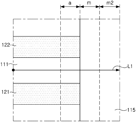
the dielectric layers and the side margin portions include Si, and an average content of Si in ‘m’ is higher than an average content of Si in ‘a’ and an average content of Si in ‘m2,’ in which ‘a’ is a region from a boundary between the active portion and the side margin portions to a region spaced apart from the boundary toward the active portion by 3μm, ‘m’ is a region from the boundary between the active portion and the side margin portions to a region spaced apart from the boundary outwardly of the side margin portions by 3μm, and ‘m2’ is a region from ‘m’ to a region spaced apart from ‘m’ outwardly of the side margin portions by 3μm,
Dm/Da is greater than 0.5 and less than 1.5 in which Da is an average size of dielectric grains in ‘a’ and Dm is an average size of dielectric grains in ‘m,’ and
the average size of dielectric grains in ‘m’ is different than an average size of dielectric grains in ‘m2’.
|