| CPC H01G 4/248 (2013.01) [H01G 4/008 (2013.01); H01G 4/012 (2013.01); H01G 4/1227 (2013.01); H01G 4/232 (2013.01); H01G 4/30 (2013.01)] | 17 Claims |
|
1. A multilayer ceramic electronic component comprising:
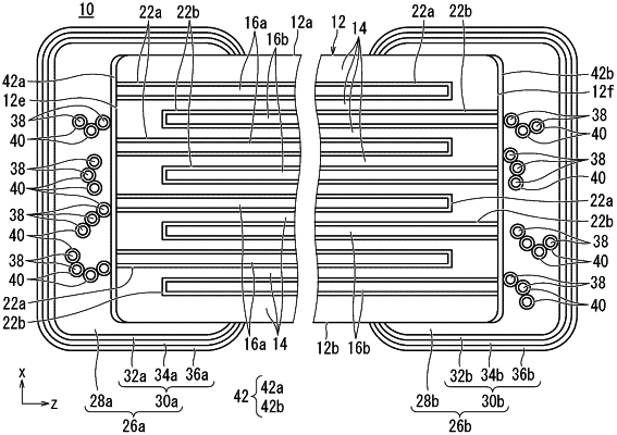
a multilayer body including a plurality of first and second ceramic layers that are stacked, a first main surface and a second main surface that face each other in a height direction, a first side surface and a second side surface that face each other in a width direction orthogonal or substantially orthogonal to the height direction, and a first end surface and a second end surface that face each other in a length direction orthogonal or substantially orthogonal to the height direction and the width direction;
a first internal electrode layer on each of the first ceramic layers and exposed on the first end surface;
a second internal electrode layer on each of the second ceramic layers and exposed on at least one surface of the second end surface, the first side surface, and the second side surface;
a first external electrode connected to the first internal electrode layer and disposed on the first end surface; and
a second external electrode connected to the second internal electrode layer and disposed on the at least one surface on which the second internal electrode layer is exposed; wherein
the first external electrode includes a first underlying electrode layer and a plurality of first plating layers located on the first underlying electrode layer;
the second external electrode includes a second underlying electrode layer and a plurality of second plating layers located on the second underlying electrode layer; and
the first underlying electrode layer and the second underlying electrode layer each include Ni as a first metal component, Sn as a second metal component, and a ceramic material; and
each of the first and second underlying electrode layers includes an alloy portion that is provided around the ceramic material and includes an alloyed Ni as the first metal component and an alloyed Sn as the second metal component.
|