| CPC H01F 17/0013 (2013.01) [H01F 27/2804 (2013.01); H01F 27/32 (2013.01); H01F 41/041 (2013.01); H05K 3/12 (2013.01); H01F 2017/004 (2013.01); H01F 2027/2809 (2013.01)] | 20 Claims |
|
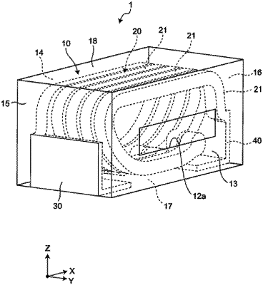
1. An inductor component comprising:
an element body, the element body including a plurality of insulating layers and a mark layer constituting a portion of an outer surface of the element body, the plurality of insulating layers and the mark layer containing K, and a K abundance ratio (atom %) in the mark layer being higher than a K abundance ratio (atom %) in all of the plurality of insulating layers;
a helically wound coil disposed in the element body; and
an external electrode disposed in the element body and electrically connected to the coil,
wherein the plurality of insulating layers each contains an amorphous intra-insulating-layer base material, and
the mark layer includes an amorphous intra-mark-layer base material and an intra-mark-layer crystal containing at least one or more pigments.
|