Memory system and operating method of the memory system
Chang Kyun Park, Gyeonggi-do (KR); Young Sik Koh, Gyeonggi-do (KR); Seung Jin Park, Gyeonggi-do (KR); and Dong Hyun Lee, Gyeonggi-do (KR)
Assigned to SK hynix Inc., Gyeonggi-do (KR)
Filed by SK hynix Inc., Gyeonggi-do (KR)
Filed on May 26, 2022, as Appl. No. 17/825,837.
Application 17/825,837 is a continuation of application No. 16/992,424, filed on Aug. 13, 2020, granted, now 11,404,097.
Application 16/992,424 is a continuation in part of application No. 16/895,050, filed on Jun. 8, 2020, granted, now 11,170,831, issued on Nov. 9, 2021.
Application 16/895,050 is a continuation in part of application No. 16/727,282, filed on Dec. 26, 2019, granted, now 11,133,080, issued on Sep. 28, 2021.
Application 16/727,282 is a continuation in part of application No. 16/679,561, filed on Nov. 11, 2019, granted, now 11,062,742, issued on Jul. 13, 2021.
Application 16/679,561 is a continuation in part of application No. 16/679,582, filed on Nov. 11, 2019, granted, now 11,069,387, issued on Jul. 20, 2021.
Application 16/679,582 is a continuation in part of application No. 16/679,601, filed on Nov. 11, 2019, granted, now 11,150,838, issued on Oct. 19, 2021.
Application 16/895,050 is a continuation of application No. 16/215,981, filed on Dec. 11, 2018, granted, now 10,714,162, issued on Jul. 14, 2020.
Claims priority of application No. 10-2019-0047421 (KR), filed on Apr. 23, 2019; application No. 10-2019-0050591 (KR), filed on Apr. 30, 2019; application No. 10-2019-0050617 (KR), filed on Apr. 30, 2019; and application No. 10-2019-0064089 (KR), filed on May 30, 2019.
Prior Publication US 2022/0284937 A1, Sep. 8, 2022
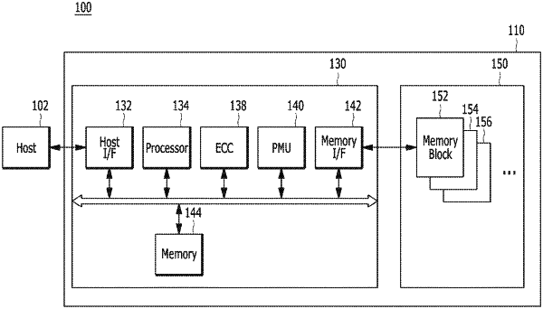
a memory device including a plurality of memory cells; and
an interface circuit configured to receive a command from a controller and perform a blocking operation to block transfer of a signal related to the command between the interface circuit and the memory device,
wherein the command is for increasing accuracy of a duty cycle.