| CPC G11C 7/1069 (2013.01) [G11C 7/22 (2013.01); G11C 8/10 (2013.01)] | 27 Claims |
|
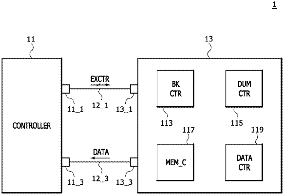
1. A semiconductor device comprising:
a memory core circuit configured to generate core data from bank data outputted by a bank or generate the core data from a dummy column address based on a read operation for the bank; and
a data control circuit configured to:
generate a switching signal from a bank active signal or a dummy bank address based on the read operation for the bank, and
control the output of the core data based on the switching signal,
wherein the core data based on the dummy column address when the read operation is not performed for the bank.
|