| CPC G11C 7/1063 (2013.01) [G11C 7/109 (2013.01); G11C 7/1012 (2013.01); G11C 7/14 (2013.01); G11C 8/18 (2013.01)] | 19 Claims |
|
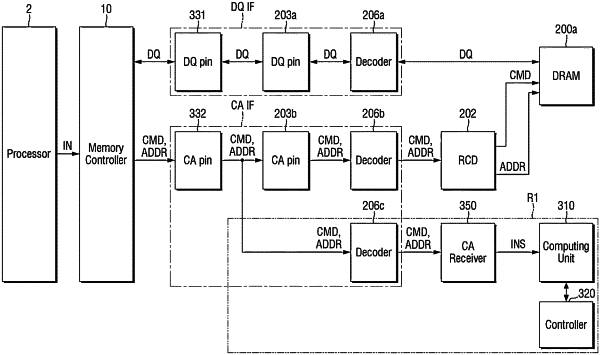
1. A semiconductor device comprising:
a data pin configured to transmit a data signal;
a command/address pin configured to transmit a command and an address;
a command/address receiver circuitry connected to the command/address pin;
a processor connected to the command/address receiver circuitry; and
a memory device connected to the data pin and the command/address pin,
wherein the command/address receiver circuitry is configured to receive a first command and a first address from an outside through the command/address pin, and generate a first instruction based on the first command and the first address,
the processor is configured to receive the first instruction and perform a computation based on the first instruction, and
the memory device is configured to receive the data signal through the data pin, to receive the command through the command/address pin, to receive the address through the command/address pin, and to store the data signal based on the command and the address.
|