| CPC G11C 29/56008 (2013.01) [G11C 16/26 (2013.01)] | 20 Claims |
|
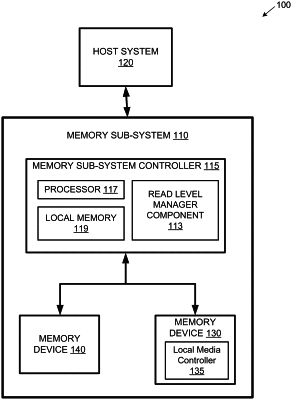
13. A system comprising:
a memory; and
a processing device communicably coupled to the memory, the processing device to perform operations comprising:
receiving a request to read data from a block of the memory;
determining a voltage distribution parameter value associated with the block of the memory, wherein the voltage distribution parameter value is based on a feature of a corresponding voltage distribution associated with a plurality of memory cells of the block; and
determining a set of read levels associated with the voltage distribution parameter value, wherein each read level in the set of read levels corresponds to a respective voltage distribution of at least one memory cell comprised by the block of the memory.
|