| CPC G11C 16/30 (2013.01) [G11C 16/0433 (2013.01); G11C 16/14 (2013.01); H03K 17/6872 (2013.01); H03K 17/693 (2013.01); G11C 2216/04 (2013.01)] | 27 Claims |
|
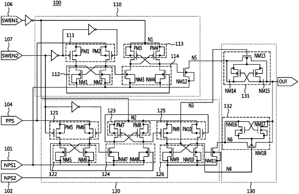
1. A negative voltage switching device, comprising:
a first switching circuit configured to transmit a first negative voltage;
a second switching circuit configured to transmit a second negative voltage; and
a switching selection circuit configured to select one of the first switching circuit or the second switching circuit for transmitting one of the first negative voltage and the second negative voltage to an output terminal, wherein the switching selection circuit comprises:
a first switching selection module connected to the first switching circuit and the second switching circuit; and
a second switching selection module connected to the second switching circuit.
|