| CPC G11C 16/10 (2013.01) [G11C 16/0483 (2013.01); G11C 16/26 (2013.01); G11C 16/30 (2013.01)] | 18 Claims |
|
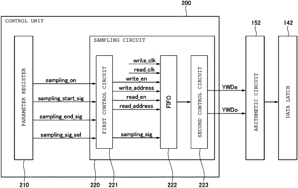
1. A semiconductor device comprising:
a first circuit including a data latch, the first circuit configured to perform writing of data to a memory using the data latch and reading of data from the memory using the data latch; and
a second circuit configured to execute a sampling process by which sampling data is collected from a predetermined node of the first circuit and stored in the data latch,
wherein the sampling process is not executed during a period in which the data latch is used for the writing of data and the reading of data.
|