| CPC G11C 16/08 (2013.01) [G11C 16/0483 (2013.01); G11C 16/14 (2013.01); G11C 16/24 (2013.01); H10B 41/27 (2023.02); G11C 16/10 (2013.01); G11C 16/26 (2013.01)] | 15 Claims |
|
1. A semiconductor storage device, comprising:
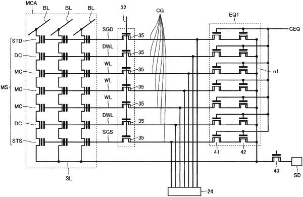
a first memory block including a first memory string including a plurality of memory cell transistors connected in series, the plurality of memory cell transistors including a first memory transistor and a second memory transistor;
a plurality of word lines connected to gates of the memory cell transistors, respectively, the plurality of word lines including a first word line connected to a gate of the first memory transistor and a second word line connected to a gate of the second memory transistor;
a first source line connected to one end of the first memory string;
a first connection transistor having one end connected to the first word line and the other end connected to the first source line; and
a second connection transistor having one end connected to the second word line and the other end connected to the first source line.
|