| CPC G11C 16/08 (2013.01) [G11C 11/5628 (2013.01); G11C 11/5642 (2013.01); G11C 16/0483 (2013.01); G11C 16/10 (2013.01); G11C 16/12 (2013.01); G11C 16/26 (2013.01); G11C 16/3459 (2013.01); H10B 43/27 (2023.02); H10B 43/35 (2023.02)] | 13 Claims |

|
1. A memory system comprising:
a semiconductor memory including:
a first block including a plurality of first memory cells;
a second block including a plurality of second memory cells;
a plurality of first word lines coupled to the first memory cells;
a plurality of second word lines coupled to the second memory cells; and
a driver circuit capable of applying voltages to the first word lines via a first row decoder and applying voltages to the second word lines via a second row decoder; and
a controller configured to control the semiconductor memory, wherein
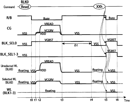
in response to a data read command for data stored in the first block or the second block, the data read command being issued by the controller to the semiconductor memory, a first voltage is applied to a selected word line, and a second voltage larger than the first voltage is applied to unselected word lines, and
in response to a first command, the first command being issued by the controller to the semiconductor memory, the driver circuit is configured to apply a third voltage smaller than the first voltage to the plurality of first word lines via the first row decoder and to apply the third voltage to the plurality of second word lines via the second row decoder.
|