US 11,915,758 B2
Memory devices with four data line bias levels
Hao T. Nguyen, San Jose, CA (US); Tomoko Ogura Iwasaki, San Jose, CA (US); Erwin E. Yu, San Jose, CA (US); Dheeraj Srinivasan, San Jose, CA (US); Sheyang Ning, San Jose, CA (US); Lawrence Celso Miranda, San Jose, CA (US); Aaron S. Yip, Los Gatos, CA (US); and Yoshihiko Kamata, Yokohama (JP)
Assigned to Micron Technology, Inc., Boise, ID (US)
Filed by MICRON TECHNOLOGY, INC., Boise, ID (US)
Filed on Jan. 10, 2023, as Appl. No. 18/095,049.
Application 18/095,049 is a continuation of application No. 17/396,825, filed on Aug. 9, 2021, granted, now 11,562,791.
Prior Publication US 2023/0162793 A1, May 25, 2023
This patent is subject to a terminal disclaimer.
Int. Cl. G11C 16/04 (2006.01); G11C 16/10 (2006.01); G11C 16/26 (2006.01); G11C 16/34 (2006.01); G11C 11/56 (2006.01)
CPC G11C 16/0483 (2013.01) [G11C 16/10 (2013.01); G11C 16/26 (2013.01); G11C 16/3459 (2013.01); G11C 11/5621 (2013.01); G11C 11/5671 (2013.01)] 20 Claims
OG exemplary drawing
 
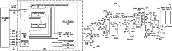
1. A memory device comprising:
a first storage element to store a first data bit;
a second storage element to store a second data bit;
a data line selectively connected to the first storage element, the second storage element, and a memory cell; and
a controller configured to apply one of four voltage levels to the data line based on the first data bit and the second data bit.