| CPC G11C 16/0483 (2013.01) [G11C 11/5635 (2013.01); G11C 16/08 (2013.01); G11C 16/10 (2013.01); G11C 16/14 (2013.01); G11C 16/16 (2013.01); G11C 16/28 (2013.01); G11C 16/3404 (2013.01); G11C 16/344 (2013.01); G11C 16/3413 (2013.01); G11C 16/3445 (2013.01); G11C 16/3463 (2013.01); G11C 2211/5621 (2013.01)] | 13 Claims |
|
1. A nonvolatile semiconductor memory device, comprising:
a memory string including a plurality of nonvolatile memory cells for data storage which are capable of storing multi-bit data connected in series,
a first dummy cell which is not used for data storage provided at at least a first end of the memory string,
select transistors connected to both ends of the memory string respectively,
word lines connected to control gate electrodes of the memory cells for data storage;
a first dummy word line connected to a control gate electrode of the first dummy cell;
a bit line connected to the first end of the memory string;
a source line connected to a second end of the memory string; and
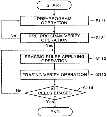
a control circuit configured to perform an erasing operation by applying an erasing voltage to the memory string,
wherein before a pre-program operation before an erasing operation to the nonvolatile memory cell, the control circuit determines whether or not a certain condition is satisfied.
|