| CPC G11C 15/04 (2013.01) | 16 Claims |
|
1. A layout of a semiconductor memory device, comprising:
a substrate; and
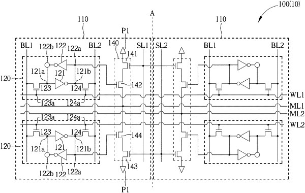
a ternary content addressable memory (TCAM), disposed on the substrate, wherein the TCAM comprises a plurality of TCAM bit cells, and at least two of the TCAM bit cells are mirror-symmetrical along an axis of symmetry, wherein each of the TCAM bit cells comprises:
two storage units, electrically connected to two word lines, respectively; and
a logic circuit, electrically connected to the two storage units, wherein the logic circuit comprises:
two first reading transistors; and
two second reading transistors, wherein each of the second reading transistors comprises a gate and two source and drain regions, and the two source and drain regions of the two second reading transistors are electrically connected to two matching lines and the two first reading transistors, respectively, wherein the word lines are disposed parallel to and between the matching lines.
|