| CPC G11C 11/5628 (2013.01) [G11C 11/4085 (2013.01); G11C 11/565 (2013.01); G11C 16/08 (2013.01); G11C 16/10 (2013.01)] | 16 Claims |
|
1. A memory system comprising:
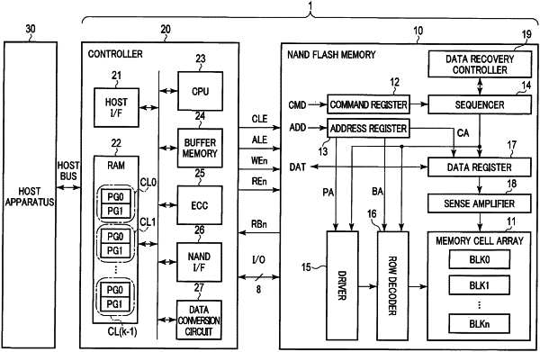
a semiconductor memory device having a first memory region including a first memory cell capable of holding at least 4-bit data and a second memory region including a plurality of second memory cells capable of holding at least 1-bit data;
a controller configured to control a first write operation and a second write operation based on the 4-bit data in the semiconductor memory device; and
at least one wiring connecting the semiconductor memory device and the controller,
wherein:
the controller includes a conversion circuit which converts the 4-bit data into n-bit data, with n being an integer,
the semiconductor memory device includes a recovery controller configured to recover the 4-bit data based on the converted n-bit data and data written in the first memory cell by the first write operation,
when the controller detects power shutdown, the conversion circuit converts the 4-bit data used for the first write operation into the n-bit data, and
the controller instructs the semiconductor memory device to write each of the n-bit data in different second memory cells of the plurality of second memory cells.
|