| CPC G09G 3/3266 (2013.01) [G09G 3/3225 (2013.01); G09G 2300/0819 (2013.01); G09G 2310/0213 (2013.01); G09G 2330/021 (2013.01)] | 19 Claims |
|
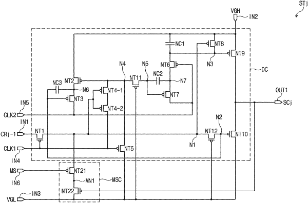
1. A scan driving circuit comprising:
a driving circuit configured to transmit a carry signal to a first node in response to a clock signal, and to output a scan signal to an output terminal in response to the clock signal and the carry signal of the first node; and
a masking circuit electrically connected between the first node and a first voltage terminal,
wherein the masking circuit comprises:
a first masking transistor configured to electrically connect the first node and a masking node in response to a masking signal; and
a second masking transistor configured to electrically connect the masking node and the first voltage terminal in response to a signal indicating an operating state of the driving circuit.
|