| CPC G09G 3/3258 (2013.01) [G02F 1/13454 (2013.01); G09G 3/20 (2013.01); G02F 2201/56 (2013.01); G09G 2300/0408 (2013.01); G09G 2300/0426 (2013.01); G09G 2310/0264 (2013.01); G09G 2310/0281 (2013.01); H10K 59/131 (2023.02)] | 20 Claims |
|
1. A non-quadrangular display, comprising:
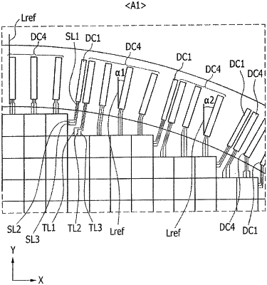
a plurality of pixels in a non-quadrangular display area, each of the pixels connected to a first signal line in a first direction and a second signal line in a second direction crossing the first direction, wherein the display area includes a curved area, the pixels are arranged in the curved area, and the curved area includes a pixel area in which pixel row steps and pixel column steps are arranged;
a plurality of first driving circuits in a peripheral area of the display area, wherein each of the first driving circuits is connected to the first signal line of a corresponding one of the pixels, and at each pixel row step a first homogenous group of the first driving circuits is arranged; and
a plurality of second driving circuits in the peripheral area of the display area, wherein each of the second driving circuits is connected to the second signal line of a corresponding one of the pixels, and at each pixel column step a second homogeneous group of the second driving circuits is arranged,
wherein a number of the first driving circuits is greater than a number of the second driving circuits, and
wherein at one of the pixel ro-w steps, the first driving circuits connected to the one pixel row step are sandwiched between adjacent second driving circuits of the column steps adjacent to the one pixel row step.
|