| CPC G06T 5/001 (2013.01) [G06T 3/40 (2013.01); G06T 9/001 (2013.01)] | 10 Claims |

|
1. An image encoding device comprising:
circuitry configured to:
generate from 3D data, 2D data including a geometry video frame, a color video frame, and an occupancy map each corresponding to the 3D data, wherein
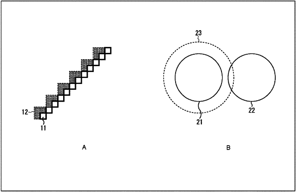
the occupancy map includes a first patch and a second patch, and
a border region of the first patch including a first blank part is overlapped with a border region of the second patch including a second blank part;
generate filtering information indicating a removal way of at least one of the first blank part or the second blank part; and
encode the 2D data and the filtering information.
|