| CPC G06F 7/5443 (2013.01) [G06F 7/523 (2013.01); G06F 17/15 (2013.01); H03M 1/46 (2013.01); G06N 20/00 (2019.01)] | 20 Claims |
|
1. An apparatus, comprising:
a plurality of data storage cells configured to store data indicative of a plurality of weights;
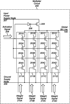
a plurality of multiplier circuits coupled to a common global bit line, wherein a given multiplier circuit of the plurality of multiplier circuits includes a plurality of device stacks including respective pluralities of devices coupled between the common global bit line and a ground supply node, wherein the plurality of device stacks are configured, in response to receiving a respective one of a plurality of activation signals indicative of a first operand, to:
receive a particular weight of a subset of the plurality of weights from the plurality of data storage cells, wherein the subset of the plurality of weights are indicative of a second operand; and
sink, based on corresponding bits included in the particular weight, corresponding ones of a plurality of currents from the common global bit line to modify a voltage level of the common global bit line; and
a first analog-to-digital converter circuit configured to convert the voltage level of the common global bit line to a plurality of bits whose value is indicative of a product of the first operand and the second operand.
|